T0 correlations in PP run 11944
Last updated: 4/16/2003 7:27 PM
TH2S *hVT0N_vs_P = new TH2S("hVT0N_vs_P","",600,1300,1900,200,1300,1900)
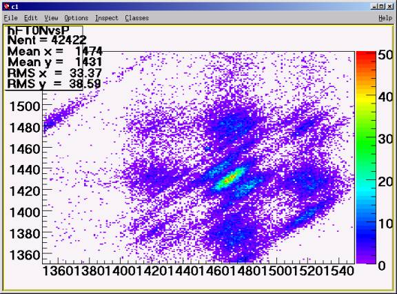
Fig. 2. FB T0N vs FB T0P
tt->Draw("TDC08[19]:TDC08[20]>>hVT0N_vs_P","1350<TDC08[19]&&TDC08[19]<1550&& 1350<TDC08[20]&&TDC08[20]<1550")
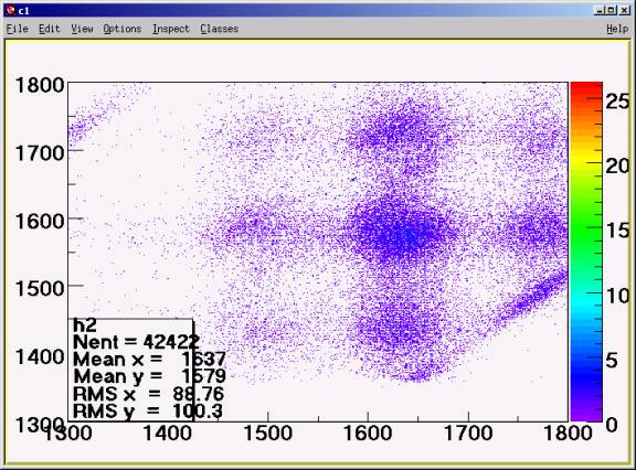
Fig. 3. VME T0N vs T0P
tt->Draw("VTDC0[1]:VTDC0[0]>>hVT0N_vs_P","1350<TDC08[19]&&TDC08[19]<1550&&1350<TD C08[20]&&TDC08[20]<1550")
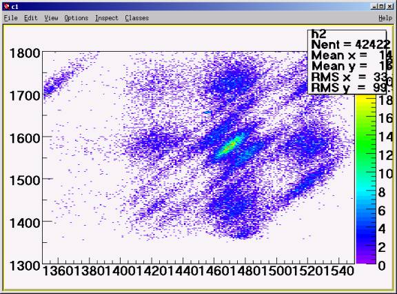
Fig 4. VME T0N vs FB T0P
tt->Draw("VTDC0[1]:TDC08[20]>>hVT0N_vs_P","1350<TDC08[19]&&TDC08[19]<1550&&1350<T DC08[20]&&TDC08[20]<1550")
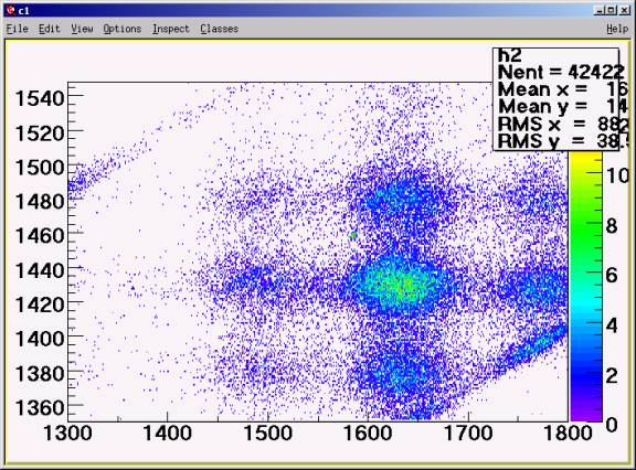
Fig. 5.
tt->Draw("TDC08[19]:VTDC0[0]>>hVT0N_vs_P","1350<TDC08[19]&&TDC08[19]<1550&&1350<
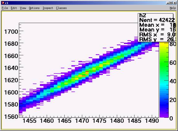
Fig. 6. VME T0P vs FB T0P
chain.Draw("VTDC0[0]:TDC08[20]>>h2","1350<TDC08[19]&&TDC08[19]<1550&&1350<TDC08[20] &&TDC08[20]<1550","colz")
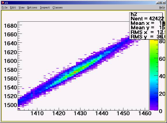
Fig. 7. VME T0N vs FB T0N
chain.Draw("VTDC0[1]:TDC08[19]>>h2","1350<TDC08[19]&&TDC08[19]<1550&&1350<TDC08[20] &&TDC08[20]<1550","colz")
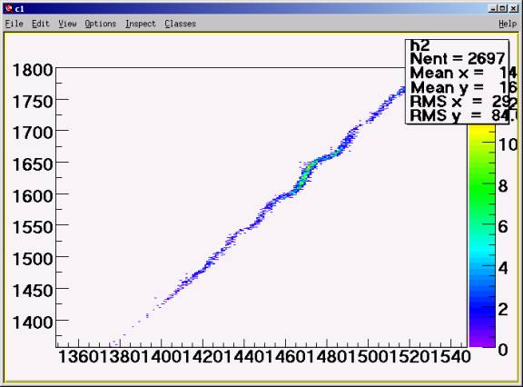
Fig. 6a. VME T0P vs FB T0P for central strip in VME T0N
chain.Draw("VTDC0[0]:TDC08[20]>>h2","1350<TDC08[19]&&TDC08[19]<1550&&1350<TDC08[20 ]&&TDC08[20]<1550&&1570<VTDC0[1]&&VTDC0[1]<1580","colz")
dAu Run 11288
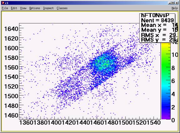
Fig. 8. Fastbus TDCs T0N vs T0P
tt->Draw("TDC08[19]:TDC08[20]>>hFT0NvsP","1450<TDC08[19]&&TDC08[19]<1650&&1350<TDC8[20]&&TDC08[20]<1550
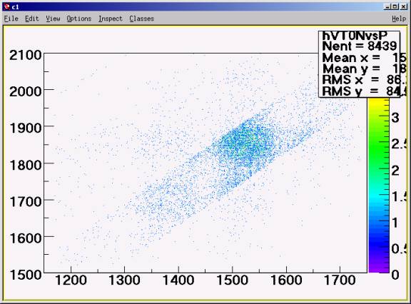
Fig. 9. VME TDCs T0N vs T0P
tt->Draw("VTDC0[1]:VTDC0[0]>>hVT0NvsP",","1450<TDC08[19]&&TDC08[19]<1650&&1350<TDC8[20]&&TDC08[20]<1550
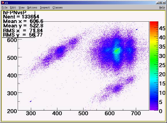
Fig. 10. PN vs PP
TH2S *hFPNvsP = new TH2S("hFPNvsP","",500,250,750,500,200,700)
chain.Draw("TDC08[32]:TDC08[33]>>hFPNvsP","","colz")
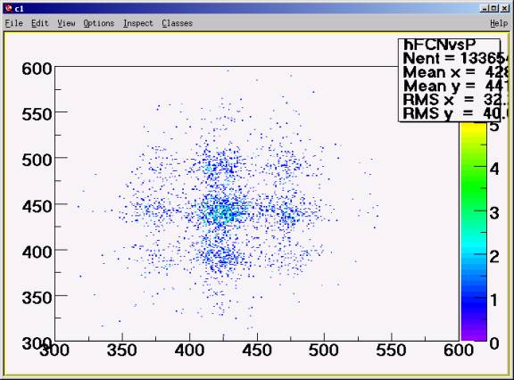
Fig. 11. CN vs CP
TH2S *hFCNvsP = new TH2S("hFCNvsP","",300,300,600,300,300,600)
chain.Draw("TDC08[16]:TDC08[17]>>hFCNvsP","","colz")
Summary:
1) The central blob in the Fastbus T0N vs T0P plot has diagonally striped structure. The stripes are separated by ~15 channels. See Fig. 2.
2) There is no such structure in the VME T0N vs T0P. See fig. 3.
3) The same structure exists in VME T0N vs Fastbus T0P (fig. 4.) and do not exist in VME T0P vs Fastbus T0N (fig. 5.)
4) Correlations VME T0N vs Fastbus T0N looks good (fig. 7.), but the same for T0P looks suspicious (fig.6)
5) The same correlations Fastbus T0N vs T0P for dAu runs does not have the diagonally striped structure fig. 8. The VME TDCs T0N vs T0P looks beautiful.
Conclusion
The striped diagonal shape in the Fastbus T0N vs T0P for PP run is due to a cross talk from T0N to T0P in the ribbon delay cable (180 ns) connecting NIM-ECL(B7) to TDC08. This cross talk is seen only in PP run because in that case both signals are coming at the same time. In the dAu run they were separated by 12 ns due to different vertex position.
Run 12045 seq. 0:3
The T0N and T0P are moved from TDC8 to TDC17 using RG58 delay cable.
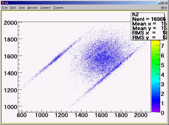
Fig. 16. VME T0N vs T0P
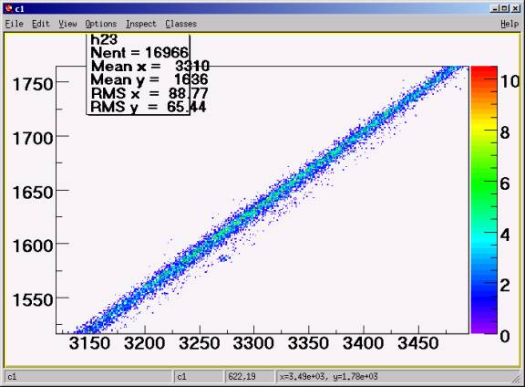
Fig. 23a. The same VTDC0[0]:TDC17[2]. The spot at x=3273,y=1586 is the time calibrator pulse. It is not obvious why it is out of band.
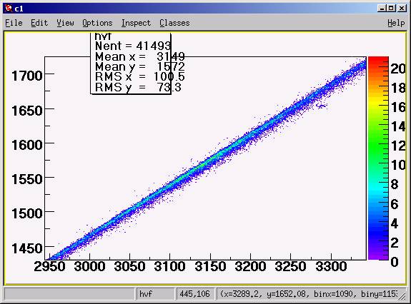
Fig. 23b. VTDC0[1]:TDC17[1]. The spot at 3289,1652 is time calibrator peak.
Problem: why the time calibrator spot is shifted from the main trace?
Which cross talk is that: VME or FastBus? One explanation - cross talk in the VME ribbon delay cable. Later it was shown that the similar blob appears with twinax cables. It is possible that TC pulse routed differently for different discriminator channels
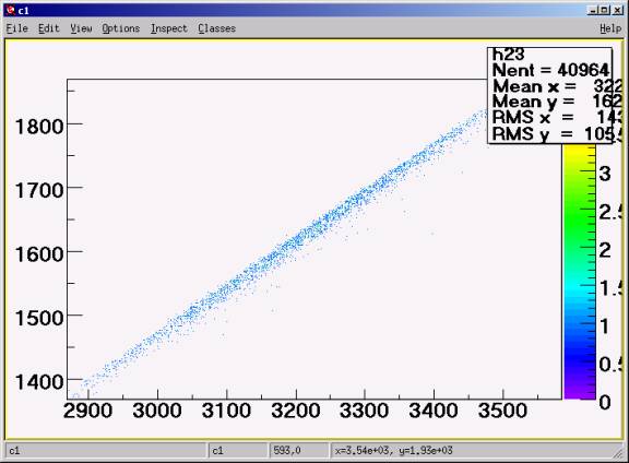
Fig. 24. VTDC0[0]:TDC17[0]. VME T0N vs T0Nx. Nice sharp left edge indicating the case when this signal have generated the OR
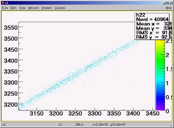
Fig. 25. TDC17[2]:TDC17[0].
Cross talk in TDC17[2]?
The upper edge is smeared. There is a problem with TDC17[2]. Compare with good shape on fig. 24 where the same signal (Y axis) is measured using VME TDC.
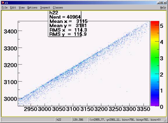
Fig. 26. TDC17[1]:TDC17[3]. Looks beautiful.
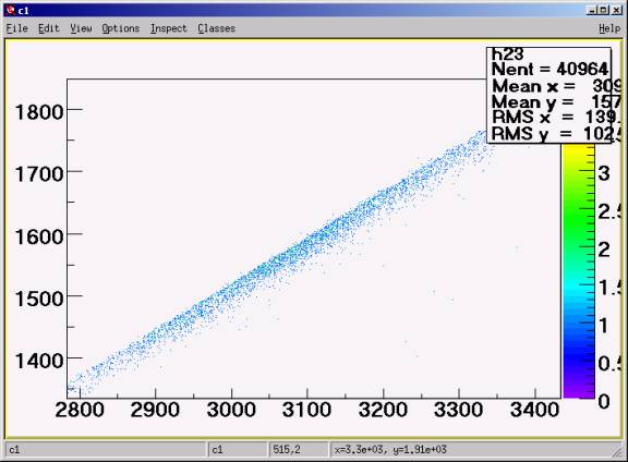
Fig. 27. VTDC0[1]:TDC17[3]. Looks OK.
FBTIME runs 12071:4. Investigating shift of the Time Equalizer peak.
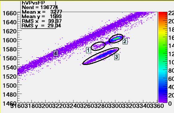
VTDC0[0]:TDC17[2].
ALLBEAM runs 12045: spots 1 and 4
FBTIME runs 12071 and 4: spot 3,
FBTIME run 12072 with only one T0P5: spot 2.
Run 12096. 4/25/2003.
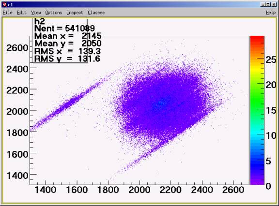
TDC17[1]:TDC17[2]
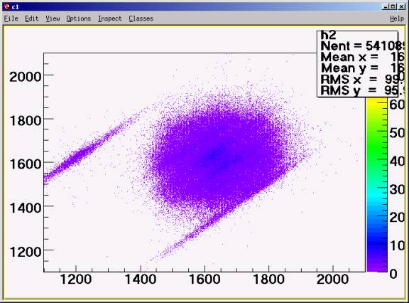
VTDC0[1]:VTDC0[0]
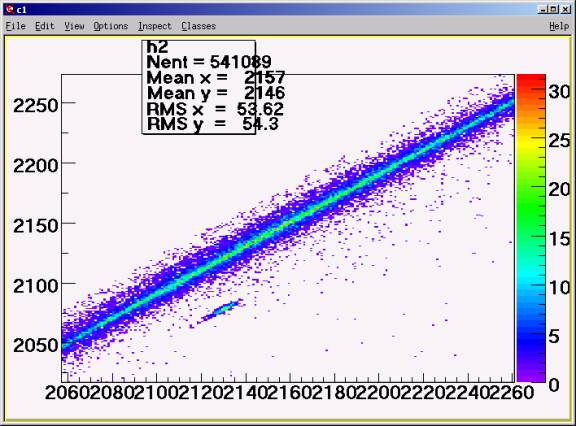
TDC17[2]:TDC17[0]. Problem1: The upper should have sharp edge with height at least 10% of the total sum. Problem 2: TC blob should be on the main strip. Possible explanation – the route for TC signal is different for different discriminator channels.
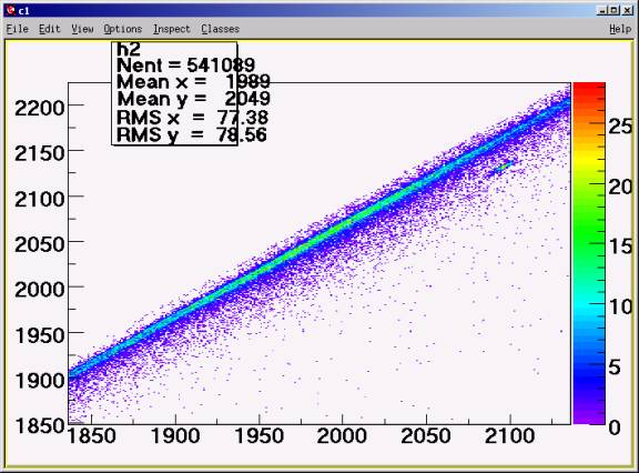
TDC17[1]:TDC17[3]. Looks good. The splitting is probably due to not perfectly aligned TEQ channels.
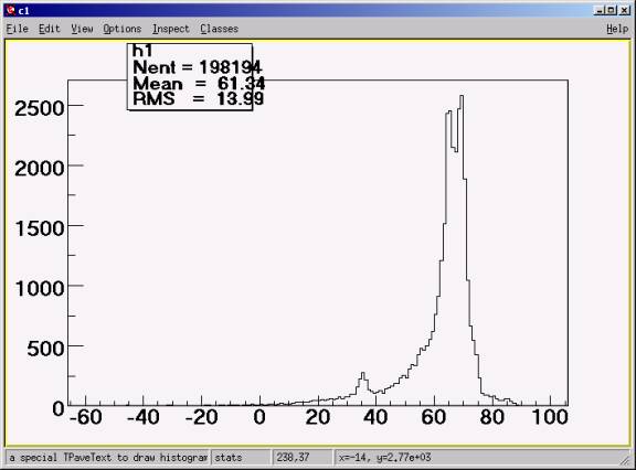
TDC17[1]-TDC17[3]
1950<TDC17[1]&&TDC17[1]<2150
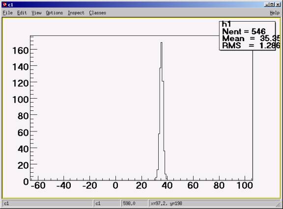
TDC17[1]-TDC17[3]
1950<TDC17[1]&&TDC17[1]<2150&&(TrigL0Latch&0x200)>0
If only TC events are selected then TC peak is beautiful.
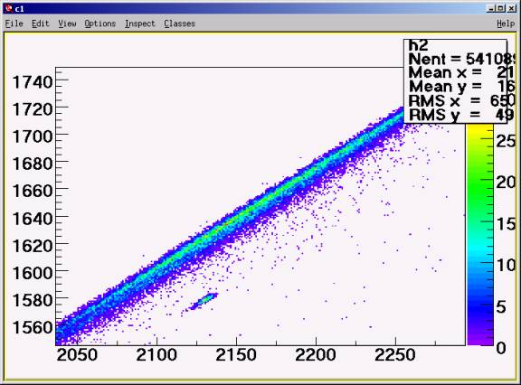
VTDC0[0]:TDC17[0]
Runs 12176:12183. Shifts in TC run with twinax cables
TDC17[1]: T0N OR from TEQ
TDC17[2]: T0P OR from TEQ
TDC17[0]: T0P0 after TEQ
Run 12176: All on
Run 12177: Only T0P0 enabled from T0P, All T0N enabled
Run 12178: Only T0P0 enabled from T0P, only T0N0 enabled in T0N
Run 12179: Only T0P0 enabled from T0P, only T0N9 enabled in T0N
Run 12180: Only T0P0 enabled from T0P, T0N0 through T0N4 enabled in T0N
Run 12181: Only T0P0 enabled from T0P, T0N5 through T0N9 enabled in T0N
Run 12182: Only T0P0 enabled from T0P, All T0N enabled
Run 12183: All on
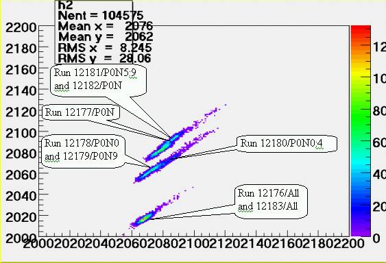
TDC17[2]:TDC17[0]
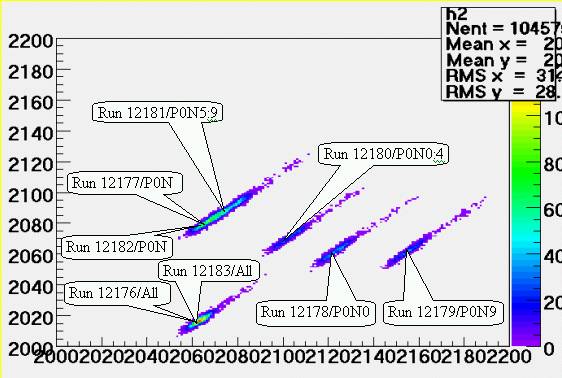
TDC17[2]:TDC17[1]. The horizontal shifts in 3 spots on the
right are due to different contribution from individual P0N channels to the T0N
OR, this is acceptable. The vertical shift for lower spot is also acceptable.
The problem is with the vertical shift between upper spot and 3 right spots.
The same conditions on T0P but changing something on T0N causes shifts in T0P0.
The common rule: the signal which comes later gets bigger shift.
Summary: The position of the T0P when only T0P0 is enabled depends on which channels in T0N are firing.
Compare runs 12177 and 12181 to runs 12178,79,80. The latter shifted down by 0.5 ns.
This is clear evidence that T0P is affected by T0N. From other hand the T0N seems to be not affected by T0P.