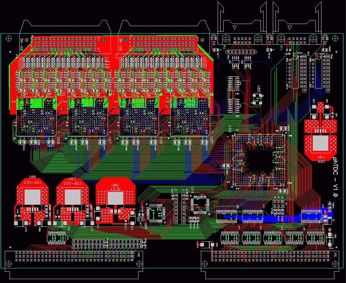
Schematic drawing of the PhTDC is ready.
Design of the PCB layout for PhTDC has started. It will take 1 month to finish.
Search for most critical components of the PhTDC is finished.
The maximum lead-time is 4 weeks.
Design of the PCB layout for PHTDC is finished. The picture is here.
Paperwork for obtaining visa for Sergei and Alexei have started.
We are ready to place an order for PCB manufacturing.
Installed Xilinx ISE 5.2. Fortunately it supports our XCV300E chip and is free.
The Xilinx programming has started.
The first version of the FPGA design have been successfully synthesized and routed. Implemented are the VME interface and the memory. It constitutes about 75% of project resources and about 25% of the logic. The design occupies ~ 25% of the chip’s resources.
According to Jorgen Christiansen, the HPTDC chips are planned for testing at CERN on the first week of September, it will be ready for delivery on the second week of September.
The funding for PhTiMeS has been approved. We can prepare the POs using capital account.
The preliminary version of the FPGA design with correct pin assignment is finished. Files are, as usual, at http://www.bnl.gov/phobos/Detectors/DataAcquisition/PhTiMeS/phtdc/phtdcx.zip
Components for PhTDC resolved. Only 3 components have lead time 2-4 weeks, Lois is ordering them. The Excel file is at http://www.bnl.gov/phobos/Detectors/DataAcquisition/PhTiMeS/phtdc/components.zip
Requested quotation for assembly from Flextronics. This will be combined order from Multek for photoplotting and Flextronics for assembly.
The minor mistake have been in phtdc.sch. The phtdcs design will be modified by Aug. 25.