Three versions of the BRAHMS receiver board will be implemented in order to satisfy various constraints for testing the board and the TPC. The first version will likely be a large 6U VME board (not standard size) and will only support VME16 and VME32. This will provide a prototype for testing the TPC. The second version will have the full functionality including support for PCI and should be a standard size 6U VME board (depending on the success of the prototype FPGA). The final (production) version of the board will be a minor rework of the 2nd board and will include fixes to discovered bugs.
Some considerations affecting the design of the board are:
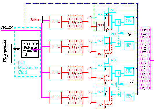
The tasks performed by the BRAHMS receiver board can be divided into a 3 stage pipeline:
Event readout will begin upon the receipt of Event Start. The 20 bits of data (High and Low words) that is received from the link will be distributed to 4 processing units. Two processing units are dedicated to each word and each word is toggled between one of two units. The DAQ is responsible for the synchronization of event readout and will only re-arm the Trigger Supervisor (TS) at appropriate time and therefore the receiver board should not receive an event start at an inappropriate time. The DAQ only re-arms the TS if readout is not in progress and if a data buffer is available. Any deviation of this policy by the DAQ will result in unexpected behavior.
Upon the completion of event readout the data that reside in the data SRAMs are sorted and consecutive memory locations hold sorted data from the same channel. To simplify the design the header words will be treated the same as data. A pedestal value of 0 will be allocated for the header words. The header words will be processed by the VME processor and part of this data will be included in the final formatted banks.
Once an entire event is sorted and buffered the RDOC bit in the status word is set, indicating that event readout is complete. The receiver processor is interrupted at this point if the RDOC bit in the interrupt enable register is set. Pedestal suppression of the data can be started if the previous event has been fully processed.
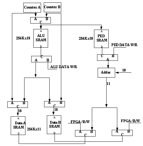
Since consecutive data over the link does not correspond to data from the same channel the pedestal subtracted data is sorted and stored in buffers (data SRAMs) before pedestal suppression. The sequence in which data is received from the readout boards is predetermined and does not change. The first 64 words over the link consists of header words and are stored into the first 32 locations of OC/EC data SRAMs (only the Low word actually contains the header words). The data is sent over the link in the same order for all time bins and the data is sorted in that order. For example if the first LOW data word (not including header) that is sent over the link corresponds to the first time bin of channel 777 then the 577th (1152/2+1) LOW data word received from the link corresponds to the 2nd time bin of channel 777. The data is sorted into data SRAMs starting at address 32 (right after header words). In the above example, the first time bin of channel 777 will reside in address 32 and the second time bin (corresponding to the 577th LOW data word) will reside at address 33. If the second LOW data word corresponds to channel 743 then the first time bin for channel 743 will be stored at address 608(609th entry)...
Two different designs are being considered to perform the pedestal subtraction and sorting of the data. In the first prototype board all 4 processing units will have a more conventional implementation (method 1) where more than 30 chips are used to implement each unit. The first board will also have one FPGA (method 2) that can replace one of the 4 processing units when appropriate jumpers are applied on the board, this is to test the feasibility of using FPGAs to reduce the size of the board in the next iteration of the board.
The pedestal values are generated by a VME processor by taking pedestal runs (by loading the pedestal values with 0x3ff) and processing the data to determine pedestal values. Lookup tables to sort the data will also be generated by the DAQ and loaded into the receiver boards before any event is read by the receiver board and after every VME reset.
This chip performs all the tasks implemented in the first method. The only difference is the use of one pedestal value per channel implemented on this chip, rather than one pedestal per bin that was used above. The limitation of pedestal values to one per channel should not adversely affect the data since it is expected that the pedestal values for each channel are approximately constant over all bins except for those on the boundaries. The boundary condition can be taken care of by the dedicated VME processor or a two level pedestal value may be implemented with lower resolution. If neither solution proves satisfactory in TPC tests, external SRAM chips can be added to provide pedestal values. A 288x11 bit synchronous SRAM is implemented on this chip to store pedestal values. 11 rather than 10 bits are used to store pedestal values to enable the retention of data with a 0 value. The Address lookup table used for sorting the data above is replaced by counters, comparators, shift registers, and additional logic, all implemented on this chip.
A test mode may also be implemented where the chip will write a programmed sequence of data to the SRAM without any actual interface to the readout board or the rosebud board. To enable this mode the clk input should be selectable to either come from the sync clock from the link or an external clock via jumpers? In this mode eventStart,... and eventEnd will be simulated by VME writes to the DFPGA. This as yet has not been implemented and depends on availability of logic gates on the chip.
Required Hardware for method 2:
	1 Xilinx XC4010-1PQ208C
	6 256K x 4 bit 12ns SRAM (also used in method 1)
	  (should be replaced by 3V, preferably wider SRAMS in next
	   version of the board to reduce chip count and cost)
	1? Delay chip used for strobing SRAMs
	1? OR chip
The following are assigned I/O pins for this chip:

Signal Name	 I/O	Description
-----------	 ---	-----------
CLK 		INPUT	link clock
datain(9:0) 	INPUT	Data from link
DataStrobe	INPUT	Input data valid
eventStart	INPUT	Indicates Start of Event
eventEnd	INPUT	Indicates End of Event
header	 	INPUT	indicates header data
resetINP 	INPUT	resets the chip
done		OUTPUT	high indicated RDOC
ready		OUTPUT	high indicates FPGA ready to accept new event
oddEvent	INPUT	high indicates the event is to be written to odd SRAM
Eaddress(17:0)	OUTPUT	address for Even Data SRAM
Oaddress(17:0)	OUTPUT	address for odd Data SRAM
Edataout(10:0)	OUTPUT	data for Even Data SRAM
Odataout(10:0)	OUTPUT	data for Even Data SRAM
Error(1:0)	OUTPUT	error code
ChipSelect	INPUT	indicates VME R/W access when high
VMERead		INPUT	When ChipSelect is high
			indicates VME read access when VMERead is high, and
			write access when VMERead is low
ChipAddr(1:0)	INPUT	Address of registers in the Chip:
			00(R/W):internal Pedestal SRAM
			01(R/W):Number of channels of Receiver board being read
			10(R):	Number of time bins per channel being read
			11(R/W):Reserved
VMEAcknowledge	OUTPUT	set high the cycle following ChipSelect
vme(15:0)	INOUT	vme data
outputDisable	INPUT	high requests all data and address lines to become Z
Estrobe		OUTPUT	Strobe Even data DRAM
Ostrobe		OUTPUT	Strobe Odd data DRAM
Temp1(17:0)	OUTPUT	Reserved
Temp2		OUTPUT	Reserved for testing
ResINP(8:0)	INPUT	Reserved for testing


THE FOLLOWING ARE OBSOLETE:
readSRAM	INPUT	low requests vme read of pedestals
			(should be followed by write)
setPedINP	INPUT	Low requests modification of internal pedestal SRAM
setSize		INPUT	Low request to change the number of channel
The second method (using DFPGAs) may be used in the 2nd and final version of the receiver board to implement pedestal subtraction and data sorting if the FPGA implementation proves successful on the prototype board.
NOTE:
The SRAMS should not be accessed(read permitted?) at this stage, when readout is in progress. Any attempts to modify the SRAMs at this stage will result in an error condition being reported (or Bus error??), and the write access will be dismissed (SRAMs will not be modified).
More restrictive clusters could also be implemented on the board but there should not be any need to do so since a dedicated VME processor can accomplish the same task once the data is sufficiently reduced. Pedestal suppression is performed in parallel in 4 FPGAs. The time to complete the pedestal suppression depends on the number of bins above pedestal and is less than (NumBINS+MaxBINSAP+MaxClusters*5)/FRQ ns, where:
	NumBINS		=(Number of data words)/4 + 32
	MaxBINSAP	=(Maximum (# of bins above pedestal for PFPGAi))
	MaxClusters	=(Maximum (# of clusters for PFPGAi))
	FRQ		=PFPGA clock Frequency(33-40Mhz)

if FIFOs are not filled completely while FPGAs are processing data(this will
not happen during normal data taking with the most central events).The time
to read the data over the link is greater than (64+NumBINSI)/FRQI ns, where:
	NumBINSI	=(Number of data words)/2
	FRQI		=link frequency(50-60Mhz).


Implementation:
---------------
Data is read from data SRAMs and shifted into sixteen (11 for data, 3 for address, and 2 for tag), 3 bit wide, data shift registers once per clock cycle. If the data is above pedestal, as indicated by the 11th and 12th bits of the data from the data SRAM(12th bit is set to 1 for header data), or the data is part of a cluster, no data is read in the next cycle. Instead either the output of data shift registeres are strobed into FIFOs or else the cluster header word(15 highest bits of the address of the data SRAMs plus a tag bit) is strobed into the FIFO followed by data shift register outputs in the following cycle. A 5 bit shift register containing previous pedestal indicators is used to decide whether data is part of a cluster. If a FIFO becomes full while pedestal suppression is in progress, the corresponding FPGA goes into an idle state until the fifoMT input is reset.
All 4 PFPGAs indicate their readiness by asserting the READY output. The READY output of each PFPGA is set when it is finished processing an event (DONE output) and if the corresponding FIFO is empty. The ODDRAM input indicates which data SRAM each PFPGA is to process. If ODDRAM is high the PFPGA gets its data from the odd data SRAM, otherwise it gets it from the even SRAM. Each PFPGA begins pedestal suppression of the data once the startINP input is set. Each PFPGA asserts the ASizeInhibit to enable the output of the latch that contains the total number of bins that was read for the event (latch drives countIO lines). The PFPGA registers countIO and immediately lowers ASizeInhibit which should result in the output of the latch to be tri-stated again. At this point the PFPGA will drive Xaddress and XaddStrobe (X=O or E) lines to read 12 bit (10 bits data, 1 bit pedestal indicator, and 1 bit header indicator) pedestal subtracted data from Xdata lines.
If VMERead intput to a PFPGA is high, the Chip is selected ( VME read access is made to PFPGASize_i), and the chip address lines (ChipAddr) correspond to "10", the corresponding PFPGA will place the number of words that it has written to the FIFO (following the first rising edge of clk) on the countIO lines, otherwise the countIO lines are not driven (Z asserted). The expected total number of data and header words from the link should be written to each PFPGA by making VME write accesses to PFPGAExpSize_i, which should result in writeSize input to be driven low. On the next rising edge of the clock the data on countIO lines will be registered. This size is compared to the actual number of words read from the link for each event. The Error(0) bit is set to 1 if the two numbers are not equal. Error(0) will remain set until the next event. A VME interrupt should be generated if the the Error interrupt bit is set in the interrupt register. The comparison is best made on the DFPGA, but since only one DFPGA is used for the current version of the receiver board the comparison is made on the PFPGAs.
The wroteKs output of the FPGA indicates that a user programmable number of words words were written to the FIFO. The HALFFIFO bit of the status word should be set the first time an FPGA asserts this signal and a VME interrupt asserted if the corresponding interrupt bit is enabled.
Required Hardware
	4 Xilinx XC4008-1PQ208C
	1 Crystal osc. as input clock
	1? Delay chip used for strobing FIFO/SRAMs
	1? OR chip

The following are assigned I/O pins for this chip:

Signal Name	 I/O	Description
-----------	 ---	-----------
OAddress(17:0)	OUTPUT	address for Odd Data SRAM
EAddress(17:0)	OUTPUT	address for Even Data SRAM
ODDRAM		INPUT	hi indicates the event is to be written to odd SRAM
clk		INPUT	input clock
clk2	 	INPUT	Reserved
data(11:0)	INPUT	data from data SRAM
fifoFull	INPUT	fifo FULL output of the FIFO
fifoMT		INPUT	fifo Empty output of the FIFO
resetINP 	INPUT	resets the chip
READY		OUTPUT	indicates the FPGA is ready to process event
startINP	INPUT	request to start processing next event
Done		OUTPUT	indicates the FPGA is done processing last event
Error(1:0)	OUTPUT	Error code
fifoData(15:0)	OUTPUT	fifo Data
fifoStrobe	OUTPUT	fifo write Strobe
getNext		OUTPUT	Obsolete
ChipSelect	INPUT	indicates VME R/W access when high
VMERead		INPUT	When ChipSelect is high
			indicates VME read access when VMERead is high, and
			write access when VMERead is low
ChipAddr(1:0)	INPUT	Address of registers in the Chip:
			00(R/W):Expected event size
			01(R/W):Minimum Number of words written to FIFO
			    	before asserting wroteKs
			10(R):	Total number of words written to FIFO
			11(R/W):Reserved
VMEAcknowledge	OUTPUT	set high the cycle following ChipSelect
countIO(19:0)	INOUT	vme data IN/OUT(20 bits) & last event size (18 bits)
ASizeInhibit	OUTPUT	Inhibit last event size output
wroteKs		OUTPUT	Indicates the FPGA has written a minimum # of words to the FIFO
Temp1(17:0)	OUTPUT	Reserved
Temp2(15:0)	OUTPUT 	Reserved
ResINP(8:0)	INPUT	Reserved for testing


THE FOLLOWING ARE OBSOLETE:
countDisable	INPUT	indicates VME read when low:
			  Assert count on countIO
ignorePed	-	IGNORE
			indicates data is to be kept regardless of
			the ped indicator. This is the 12th bit of (O/E)data
			which is 1 for header data. ONLY FOR 1ST PROTOTYPE
writeSizeN	INPUT	Indicates VME write access when low:
			  write the expected size when countIO(19:18)="00"
			  write the MinWords when countIO(19:18)="01"
Pedestal suppressed data is written to 4 FIFOs (one for each FPGA, 16K deep) asynchronously. The size of data that has been processed but not suppressed (including header words) is available as pedestal suppression proceeds and can be accessed from VME by reading the PFPGASize_i registers. If the HALFFIFO interrupt bit is enabled, the receiver board asserts a VME interrupt indicating that at least one of the four FPGAs has written a minimum number of words (MinWords, see dsefinitions below) to its FIFO. This interrupt may be asserted only once per event, the first time one of the PFPGAs has exceeded outputting the minimum number of words. Upon the receipt of this interrupt the PFPGASize_i registers should be read to determine the number of words written by each PFPGA and data readout should be initiated. This should be done to maximize the DAQ rate especially when taking pedestal data, since once a FIFO is full the corresponding PFPGA will suspend until there is space in the FIFO. Data will be available for readout from each FIFO and can be accessed from VME (using A32/D32) asa the FPGAs start processing the data. FIFO data can only be accessed two words (32 bits) at a time in long words. Since two words are packed into one long word when data is read from the FIFO, the number of reads should be half of PFPGASize_i. No attempt should be made to read the fifo if there is only one word in the fifo except to read the last word after PFPGAs have completed processing the whole event.
What happens if an attempt is made to read an empty buffer?
The final receiver board will automatically initiate data transfer to a dedicated VME processor using PCI.
Cluster TAGS:
DFPGA_SRAM_i(i=1,2,3,4): FPGA ped SRAM. The pedestal values should be written to each FPGA pedestal SRAM (at least) once after VME reset and when pedestal values change. Modification of pedestal values require two VME accesses, the first access indicates the address, and the second access indicates the pedestal value. The required two accesses reduce the number of pins used on the FPGA (also reduce the number of bus lines on the receiver board).
PFPGASize_i (i=1,2,3,4): Number of 16 bit data words written to FIFO by the PFPGA_i. This register can be read while the PFPGA is processing the data. PFPGASize indicates the total number of pedestal suppressed data words for the event for PFPGA_i and includes the header words.
PFPGAExpSize_i (i=1,2,3,4): Number of data bins to be processed by the FPGA. This should be written to each FPGA (at least) once after VME reset. This number should be 64/2 + (NumChannels*Number of bins)/4
DFPGANumBins_i (i=1,2,3,4): Number of bins per channel. This should be written to each DFPGA (at least) once after VME reset.
DFPGANumChans_i (i=1,2,3,4): Number of channels to be processed by the DFPGA (data readout FPGA). This should be written to each FPGA (at least) once after VME reset. DFPGANumChans_i=NumChannels/4
MinWords: Number of words written to FIFOs before PFPGAs assert their wroteKs output (which may result in a VME interrupt). This is user programmable and should be written to each PFPGA (at least) once after VME reset. To write MinWords, write each PFPGAExpSize_i with binary 01xxxxxxxxxxxxxxxxxx where x's refertype checkFinishFSM_type is (S_F_idle,S_F_check);
signal checkFinishFSM:checkFinishFSM_type;
type startFSM_type is (S_S_idle,S_S_go);
to the binary representation of the minimum number of words.
VME interrupts are supported by the receiver board. Four possible sources of interrrupts can be enabled/disabled individually by setting the appropriate bits in the INTENABLE register. Two registers, INTLEVEL and INTVECTOR, should be configured to set the VME interrupt level and vector. The sources of interrupts are RDOC, HALFFIFO, FPGADONE, and ERROR:
RDOC(ReaDOut Complete): If the corresponding interrupt bit is enabled, the receiver board asserts a VME interrupt indicating the completion of event readout. This will occur once an event is fully readout and sorted into the data SRAM. This does not indicate that pedestal suppression has been performed, nor does it indicate that the TS can be re-armed. The RDORDY bit should be checked to re-arm the TS.
FPGADONE: If the corresponding interrupt bit is enabled, the receiver board asserts a VME interrupt indicating all 4 PFPGAs have completed pedestal suppression.
HALFFIFO: If the corresponding interrupt bit is enabled, the receiver board asserts a VME interrupt indicating at least one of the four FPGAs has written a minimum user programmable number of words to its FIFO. This interrupt may be asserted once per event, the first time one of the PFPGAs has exceeded outputting the minimum number of words (not once for each FPGA). Upon the receipt of this interrupt the PFPGASize_i registers should be read to determine the number of words written by each PFPGA and data readout should be initiated. This should be done to maximize the DAQ rate especially when taking pedestal data, since once a FIFO is full the corresponding PFPGA will suspend until there is space in the FIFO. Since two words are packed into one long word when data is read from the FIFO the number of reads should be half of PFPGASize_i.
ERROR: If the corresponding interrupt bit is enabled, the receiver board asserts a VME interrupt indicating an error condition. The Error register should be read to determine the source of the error and appropriate action should be taken.
Header: 1xaaaaaaaaaaaaaa        (x is the highest address bit and is always 0 for BRAHMS)
Data:   01aaapdddddddddd

bits 15:14      bits(13:11)     bit 10                          bits 9:0
----------      -----------     ------                          --------
01 Data tag     address 2:0     pedestal indicator:             ped. subtracted
                                0 if data below pedestal        data
                                1 if data above pedestal

1x tag/header   header          header                          header
   address 17*  address 16:14   address 13                      address 12:3

00 Undefined

* Since only ~128 time bins will be used for BRAHMS' TPC readout the highest
address bit will always be 0.

***Exception:
The first cluster which contains the 32 header words, start with a header
(0x8000) followed by two extra words, followed by 32 words, and followed by a
 minimum of two words which correspond to the first two bins of the first
channel. The first extra word consists of a 16 bit event number. The second
extra word is set to 0. The first header word is thus the fourth word written to the FIFO. -------Sorry for two different kinds of headers

EXAMPLE:
The following data starting at address 0x7000 in data SRAM:
"Address"       ~Pedestal       value
-------         --------        -----
0x7000          0               0x0
0x7001          0               0x3fd
0x7002          1               0x100
0x7003          1               0x100
0x7004          1               0x100
0x7005          1               0x100
0x7006          1               0x100
0x7007          0               0
0x7008          0               0x3fe
0x7009          0               0
0x700a          0               0x3ff


will result in the following sequence of data after pedestal suppression
(assuming that 2 pedestal bins are kept above and below the cluster):
0x8e00
0x4000
0x4bfd
0x5500
0x5d00
0x6500
0x6d00
0x7500
0x7800
0x43fe
Final Format:VME Interface:
Access to various SRAMs and registers on the receiver board is memory mapped to extended VME address space. Each receiver board occupies 16MB of continous address space. The base address of each board is settable on the board by a set of 8 switches which correspond to the highest 8 address bits (31 to 24). Each receiver board will respond to VME16 as well as VME32 in both Supervisory and User modes. Block transfers are supported only for long word read (32 bits) access from the output FIFOs. The following is a summary of the offset and access type for access to the receiver board:
Name		Size(BITS)	Read/Write**	VME Access Size	Offset

----
ASRAM_LO_OC	256K x 18	W(R)		long		0x
ASRAM_LO_EC	256K x 18	W(R)		long		0x
ASRAM_HI_OC	256K x 18	W(R)		long		0x
ASRAM_HI_EC	256K x 18	W(R)		long		0x

PSRAM_LO_OC	256K x 10	W(R)		short		0x
PSRAM_LO_EC	256K x 10	W(R)		short		0x
PSRAM_HI_OC	256K x 10	W(R)		short		0x
PSRAM_HI_EC	256K x 10	W(R)		short		0x

DSRAM_LO_OE_OC	256K x 11	(R/W)		short		0x
DSRAM_LO_OE_EC	256K x 11	(R/W)		short		0x
DSRAM_LO_EE_OC	256K x 11	(R/W)		short		0x
DSRAM_LO_EE_EC	256K x 11	(R/W)		short		0x
DSRAM_HI_OE_OC	256K x 11	(R/W)		short		0x
DSRAM_HI_OE_EC	256K x 11	(R/W)		short		0x
DSRAM_HI_EE_OC	256K x 11	(R/W)		short		0x
DSRAM_HI_EE_EC	256K x 11	(R/W)		short		0x

FIFO_1		X x 16*		R		long		0x
FIFO_2		X x 16*		R		long		0x
FIFO_3		X x 16*		R		long		0x
FIFO_4		X x 16*		R		long		0x

PFPGASize_1	18		R		long		0x
PFPGASize_2	18		R		long		0x
PFPGASize_3	18		R		long		0x
PFPGASize_4	18		R		long		0x

PFPGAExpSize_1	18		W		long		0x
PFPGAExpSize_2	18		W		long		0x
PFPGAExpSize_3	18		W		long		0x
PFPGAExpSize_4	18		W		long		0x

DFPGANumBins_1	9		W		short		0x
DFPGANumBins_2	9		W		short		0x
DFPGANumBins_3	9		W		short		0x
DFPGANumBins_4	9		W		short		0x

DFPGANumChans_1	9		W		short		0x
DFPGANumChans_2	9		W		short		0x
DFPGANumChans_3	9		W		short		0x
DFPGANumChans_4	9		W		short		0x

DFPGA_SRAM_1	16		R/W		short		0x
DFPGA_SRAM_2	16		R/W		short		0x
DFPGA_SRAM_3	16		R/W		short		0x
DFPGA_SRAM_4	16		R/W		short		0x

STATUS		32		R		long		0x
ERROR		32		R		long		0x
ACTION		16?		W		short		0x

INTLEVEL	3		W		short		0x
INTVECTOR(s?)	8		W		short		0x
INTENABLE	4(>?)		W		short		0x
INTASSERTED	4(>?)		R		short		0x


OTHERS?

* Although the data in the FIFO is 16 bits wide, a VME access to the FIFO
results in packing two consecutive short words into a long 32 bit word,
so each single VME read from FIFO_i will result in reading two data words
from the FIFO, doubling the transfer rate.

** Parenthesis indicate options for debugging only


DEFINITIONS:
------------

DFPGA		Refers to the single prototype FPGA used for event readout
PFPGA		Refers to the FPGAs used for pedestal suppression

DSRAM_LO_OE_OC	low 10 bits of Data SRAM, for odd events, odd channels
DSRAM_LO_OE_EC	low 10 bits of Data SRAM, for odd events, even channels
DSRAM_LO_EE_OC	low 10 bits of Data SRAM, for even events, odd channels
DSRAM_LO_EE_EC  low 10 bits of Data SRAM, for even events, even channels
DSRAM_HI_OE_OC  High 10 bits of Data SRAM, for odd events, odd channels
DSRAM_HI_OE_EC	High 10 bits of Data SRAM, for odd events, even channels
DSRAM_HI_EE_OC	High 10 bits of Data SRAM, for even events, odd channels
DSRAM_HI_EE_EC	High 10 bits of Data SRAM, for even events, even channels

PSRAM_LO_OC	Low 10 bits of Ped SRAM, for odd channels
PSRAM_LO_EC	Low 10 bits of Ped SRAM, for even channels
PSRAM_HI_OC	High 10 bits of Ped SRAM, for odd channels
PSRAM_HI_EC	High 10 bits of Ped SRAM, for even channels

ASRAM_LO_OC	Add Lookup Table for Low 10 bits, for odd channels
ASRAM_LO_EC	Add Lookup Table for Low 10 bits, for even channels
ASRAM_HI_OC	Add Lookup Table for High 10 bits, for odd channels
ASRAM_HI_EC	Add Lookup Table for High 10 bits, for even channels

ERROR:
	4 bits: 2 bit for each PFPGA
	4 bits: 2 bit for each DFPGA
	1 bit:	link error
	1 bit:	abort
	1 bit:  VME access to SRAMs while processing data

STATUS:
	1 bit: RDORDY
	1 bit: RDOBSY
	1 bit: ERROR:
	8 bits: 2 for each PFPGA
	8 bits: 2 for each DFPGA
	1 bit: RDOC
	1 bit: HALFFIFO
	1 bit: FPGADONE
	1 bit: ERROR

ACTION:
	1 bit: Reset Board
	1 bit: Reset PFPGAs
	1 bit: Reset DFPGAs
	1 bit: Reset Registers
	1 bit: Reset FIFOs

RDORDY: indicates the readout board is ready to take the next event
RDOBSY: indicates the readout board is busy receiving an event from the link
ERROR:	indicates error condition
Interrupts:
Karim Ashktorab